As an undergraduate at Princeton University, I conducted research in the domain of large-area electronics under the guidance of Professors Sigurd Wagner and, in my senior year, Naveen Verma.
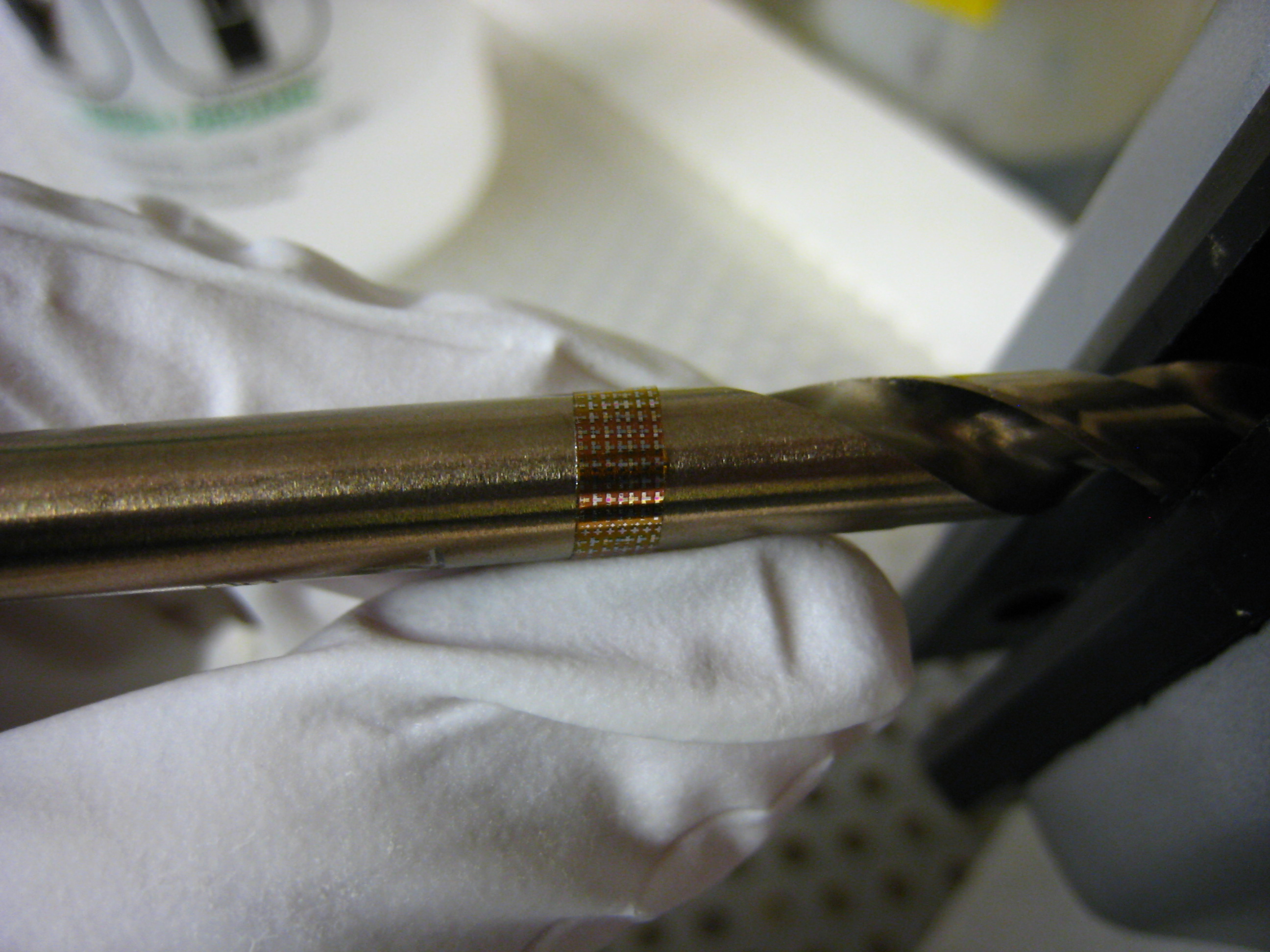
Starting in the spring of my sophomore year, my first project was to characterize the mechanical flexibility of hydrogenated amorphous silicon (a-Si:H) thin-film transistors (TFTs) that were fabricated with a new gate dielectric material that had previously been developed in the lab as an encapsulation layer for organic light-emitting diodes (OLEDs). a-Si:H TFTs are conventionally made with a silicon nitride (SiNx) gate dielectric, and while this material is generally electrically impermeable, it is also very stiff and thus limits the overall flexibility of the devices and subsequent applications (e.g. flat panel displays). The new gate dielectric is a silicon dioxide (SiO2)-silicone “hybrid” insulator that had recently been found to possess both the electrical insulation properties characteristic of inorganic materials and the mechanical flexibility of organic materials. TFTs made with the new dielectric exhibit electron mobilities of 2 cm2 / V-s - roughly twice that of conventional a-Si:H/SiNx TFTs. I found the resulting TFTs to be very flexible, recovering from tensile strains of up to 2.5% (corresponding to bending around a radius of 1 mm).

Flexible TFTs bent around a drill bit
I then fabricated and characterized TFTs made with the new dielectric in a top-gate staggered geometry. The bottom-gate staggered geometry is conventional in a-Si:H TFT research because it yields the highest electron mobility. However, the top-gate staggered geometry is of interest because it is less complex to fabricate (fewer required photolithography masks and easier to integrate into display circuitry. Furthermore, we were interested in the effect of layer growth sequence on the performance of TFTs with our new gate dielectric material. The resulting top-gate TFTs exhibited an effective electron mobility of ~0.5 cm2 / V-s, a threshold voltage of ~1.5 V, and an on-off current ratio of ~106, values that are comparable to typical average-performance a-Si:H/SiNx TFTs.
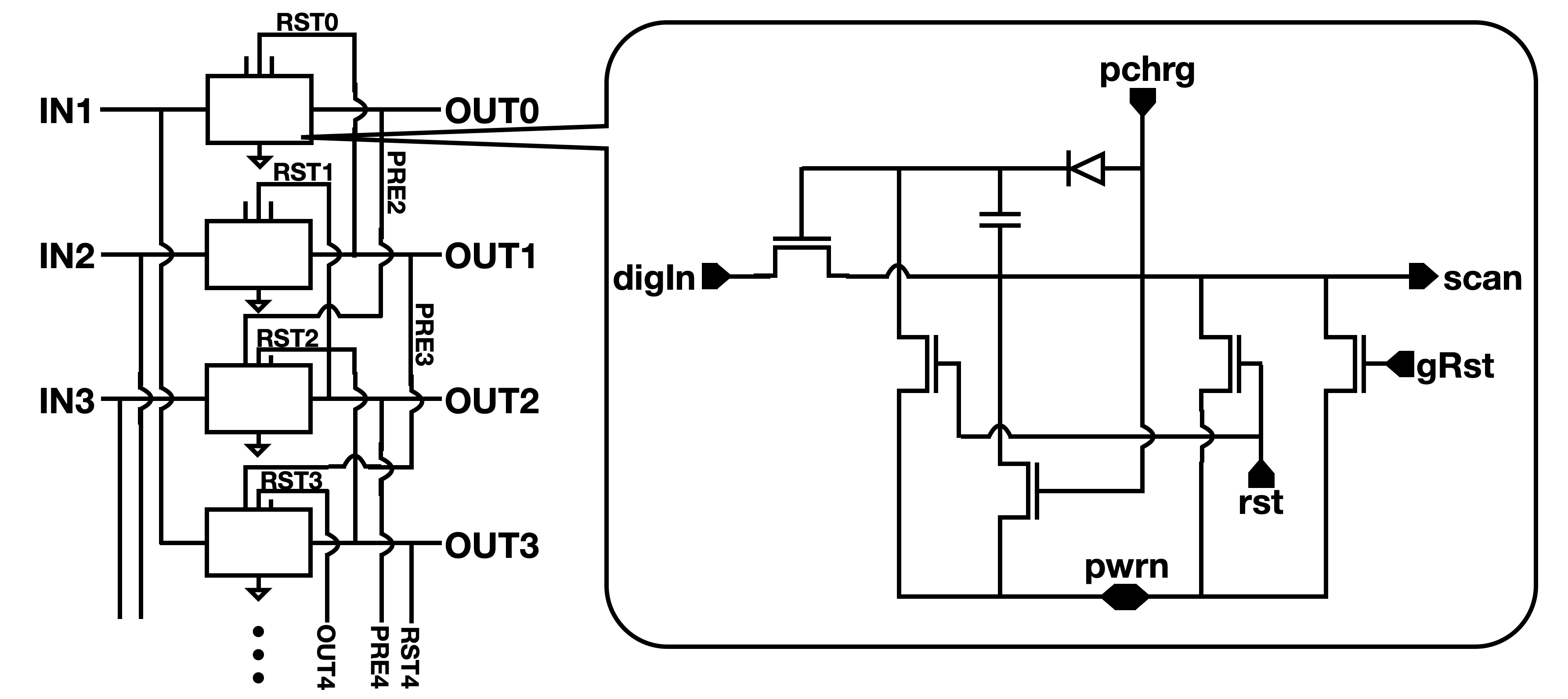
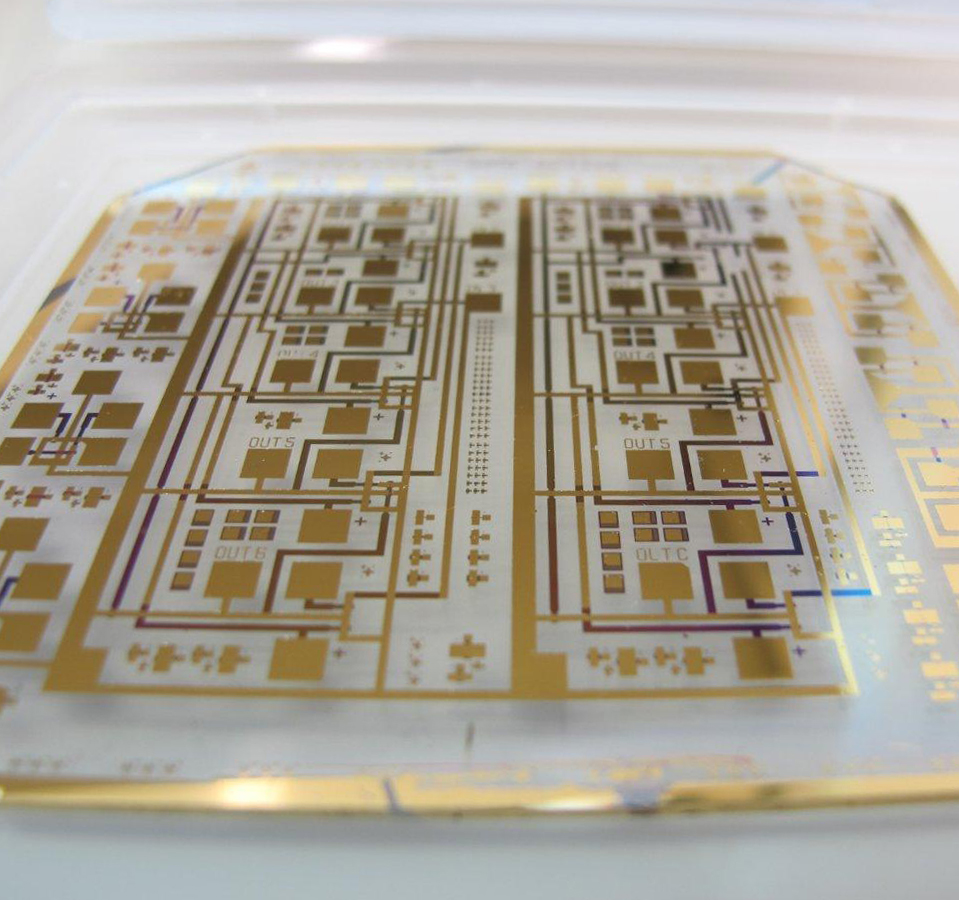
Scanning circuit schematic (left) and fabricated large-area circuits on glass
For my senior thesis, I worked with Professors Wagner and Verma to design and fabricate a dynamic a-Si:H TFT “scanning” circuit to interface between arrays of thin-film sensors and nanoscale integrated circuit chips for a system to monitor the formation and propagation of cracks on a bridge. This “hybrid” system architecture takes advantage of the high speed processing of modern ICs and the low cost, mechanical flexibility, and scalable nature of large-area electronics.
publications
-
61.3: Amorphous Silicon TFT Technology for Rollable OLED Displays
Sigurd Wagner, Lin Han, Bahman Hekmatshoar, Katherine Song, Prashant Mandlik, Kunigunde H. Cherenack, and James C. Sturm
SID Symposium Digest of Technical Papers, 2010
Amorphous silicon thin-film transistors were designed for roll-out OLED screens in hand-held devices. Separate TFTs reached a saturation current of 6 μA/square, an output current half-life extrapolating to 1,000 years, and were rolled to 1 mm diameter. All three parameters set new world records.
-
17.3: a-Si:H Thin-film Transistors with a New Hybrid Dielectric Highly Stable under Mechanical and Electrical Stress
Lin Han, Katherine Song, Sigurd Wagner, and Prashant Mandlik
SID Symposium Digest of Technical Papers, 2010
A resilient, homogeneous, hybrid of silicon dioxide and silicone polymer deposited at room-temperature replaces the conventional, brittle, silicon nitride barrier layer and gate insulator in amorphous silicon thin-film transistors(a-Si:H TFTs) on flexible polyimide foil. The electron field-effect mobility is high at 1.6 cm2/V⋅s, and the threshold voltage shift under high gate bias is comparable to that in conventional a-Si:H/SiNx TFTs fabricated at 300oC. The substhreshold slope is 290 mV/decade. The new transistors are highly flexible, as they can be bent down to 0.5 mm radius (5% strain) in tension and down to 1mm radius (2.5% strain) in compression. These TFTs qualify for roll-out screens of hand-held devices.
-
(Invited) A New Insulator for Thin-Film Transistor Backplanes and for Flexible Passivation Layers
Lin Han, Katherine Song, Sigurd Wagner, and Prashant Mandlik
In ECS Transactions, 2010
We describe a new flexible material that functions as a gate dielectric of amorphous-silicon thin-film transistors, as a passivation layer for plastic substrates, and as an environmental barrier for organic light-emitting diodes. The material is SiO2 with some silicone polymer character. It is deposited, typically at room temperature, from a glow discharge in which a silicone precursor molecule, hexamethyl disiloxane, is oxidized. Films of the material can be made with a broad range of properties, which vary from those of SiO2 to those of plasma-polymerized silicone. Many macroscopic properties of these films suggest that they are homogeneous. We call the films "hybrid."
-
Ultraflexible amorphous silicon transistors made with a resilient insulator
Lin Han, Katherine Song, Prashant Mandlik, and Sigurd Wagner
Applied Physics Letters, Jan 2010
The conventional, brittle, silicon nitride barrier layer and gate insulator in amorphous silicon thin-film transistors (a-Si:H TFTs) on 50μm thick polyimide foil was replaced by a resilient, homogeneous, hybrid of silicon dioxide and silicone polymer. The transistor structures can be bent down to 0.5 mm radius (5% strain) in tension and down to 1 mm radius (2.5% strain) in compression. This pronounced flexibility shifts the criterion for reversible bending away from a-Si:H TFT backplanes and toward the materials for substrate and encapsulation. It qualifies a-Si:H TFTs for pull-out display screens in handheld devices.
-
Effects of Mechanical Strain on the Electrical Performance of Amorphous Silicon Thin-Film Transistors with a New Gate Dielectric
Katherine Wei Song, Lin Han, Sigurd Wagner, and Prashant Mandlik
MRS Proceedings, Jan 2009
The stiff SiNx gate dielectric in conventional amorphous silicon thin film transistors (TFTs) limits their flexibility by brittle fracture when in tension. We report the effect on the overall flexibility of TFTs of replacing the brittle SiNx gate dielectric with a new, resilient SiO2-silicone hybrid material, which is deposited by plasma enhanced chemical vapor deposition. Individual TFTs on a 50µm-thick polyimide foil were bent to known radii, and measurement of transfer characteristics were made both during strain and after re-flattening. Compared with conventional TFTs made with SiNx, TFTs made with the new hybrid material demonstrated similar flexibility when strained in compression and significantly increased flexibility when strained in tension. Under bending to compressive strain, all TFTs tested delaminated from the substrate for compressive strains greater than 2%. Conventional a-Si:H/SiNx TFTs have been previously found to delaminate at a similar compressive strain. Under bending to tensile strain, the most flexible TFTs made with the new hybrid material that were tested after re-flattening did not exhibit significant changes in transfer characteristics up to strains of 2.5%. Conventional aSi:H/SiNx TFTs have been found to remain functional for strains of up to 0.5%, a value only one-fifth of that for TFTs made with the new hybrid material.
-
High-resolution sensing sheet for structural-health monitoring via scalable interfacing of flexible electronics with high-performance ICs
Yingzhe Hu, Warren Rieutort-Louis, Josue Sanz-Robinson, Katherine Song, James C. Sturm, Sigurd Wagner, and Naveen Verma
In 2012 Symposium on VLSI Circuits (VLSIC), Jun 2012
Early-stage damage detection for buildings and bridges re quires continuously sensing and assessing strain over large sur faces, yet with centimeter-scale resolution. To achieve this, we present a sensing sheet that combines high-performance ICs with flexible electronics, allowing bonding to such surfaces. The flexi ble electronics integrates thin-film strain gauges and amorphous silicon control circuits, patterned on a polyimide sheet that can potentially span large areas. Non-contact links couple digital and analog signals to the ICs, allowing many ICs to be intro duced via low-cost sheet lamination for energy-efficient readout and computation over a large number of sensors. Communi cation between distributed ICs is achieved by transceivers that exploit low-loss interconnects patterned on the polyimide sheet; the transceivers self-calibrate to the interconnect impedance to maximize transmit SNR. The system achieves multi-channel strain readout with sensitivity of 18J1’strainRMs at an energy per measurement of 270nJ, while the communication energy is 12.8pJ/3.3pJ per bit (Tx/Rx) over 7.5m.
-
Large Area Circuits for a Hybrid Macroelectronics-Nanoelectronics Active Monitoring System
Katherine Wei Song
Undergraduate Thesis (Princeton University), Jun 2011
Hydrogenated amorphous silicon (a-Si:H) thin film transistors (TFTs) are critical components for large area electronics, such as displays and sensors, but up until now, their applications in flexible electronics technology has been limited by their low degree of flexibility. Conventional a-Si:H TFTs are made with a stiff, brittle silicon nitride (SiNx) gate dielectric that restricts the overall flexibility of the devices. Recently, a new, compliant SiO2-silicone hybrid material was invented to replace the conventional SiNx in TFTs. This “hybrid” was found to possess the electrical impermeability characteristic of an inorganic SiO2 dielectric as well as the flexibility characteristic of the polymeric silicone. In the first part of this thesis, we describe studies on the flexibility of TFTs made with the new gate dielectric. We find that the replacement of the SiNx gate dielectric in a-Si:H TFTs with the SiO2-silicone hybrid material results in up to a ten fold increase in flexibility. The development of these ultra-flexible a-Si:H TFTs opens the path to new domains for electronics. In addition to being used in flexible displays, flexible a-Si:H TFTs have the potential to be implemented in new environments that are traditionally off limits to conventional electronics. Here, we describe one such application. The target application of our particular system is for structural health monitoring (SHM) of infrastructure, but it may ideally be applied to systems in other environments as well. a-Si:H TFT based large area circuits are combined with nanoscale integrated circuit (IC) chips to form a system that is both computationally efficient and scalable. The second part of this thesis focuses on a “scanning circuit” composed of a-Si:H TFTs that serves as the interface between a nanoscale IC chip and an array of large area sensors. It is designed to accommodate the low power requirements of the system and account for the imbalance between n-channel and p-channel performance in a-Si:H TFTs. The circuit is initially simulated using standard 90nm Generic Process Design Kit models, and once the functionality is confirmed, a TFT model for simulation is created by empirically fitting a SPICE Level 1 MOSFET model to measured TFT output characteristics. Circuit simulations run with this TFT model demonstrate that the scanning circuit is a feasible design in theory. Preliminary experiments on a single scanning block indicate that the circuit can operate at frequencies of 2.5 kHz, which is sufficient for the target frequency of ∼ 1 kHz.


